Simulation of pixel-size impact for optical brightfield wafer defect inspection: Difference between revisions
| Line 48: | Line 48: | ||
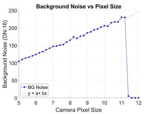
Background noise increases linearly to the pixel size. This is also expected since number of photon collected is proportional to the area. | Background noise increases linearly to the pixel size. This is also expected since number of photon collected is proportional to the area. | ||
=== Capture rates when the pixel size and effective defects size match === | |||
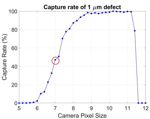
==== Sensor with 7um pixels ==== | |||
[[File: Capture rate at 7um.jpg|500px]] | |||
==== Sensor with 10um pixels ==== | |||
[[File: Capture rate at 10um.jpg|500px]] | |||
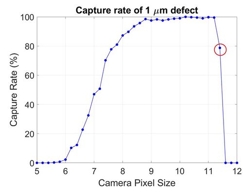
==== Sensor with 11.4um pixels ==== | |||
[[File: Capture rate at 11.4um.jpg|500px]] | |||
== Conclusions == | == Conclusions == | ||
Revision as of 05:27, 18 December 2023
Introduction
These days, we do not get by a day without technology. Yet, we hardly stop to think about the very foundations that allow our way of life: semiconductors. Notably so, as the early computers took up a huge room. Today, we hold them in our palms, and fork out hundreds or thousands of dollars to buy them. With the world revolving around digital transformation and technology, the pressure is on semiconductor manufacturers to take on ever increasing challenges of creating higher complexity chip designs, explore new processes and materials. They also have to grapple with yield loss, which is an ever-present problem.
Typically, advanced semiconductor nodes are made by combining many processes together on a silicon wafer to fabricate the dies containing the intended designs. The dies are then diced into individual chips before being packaged and shipped. As complexity grows, so does the number of processes, and thus the manufacturing steps. These are all inception points for defects, which can cause the chips to fail and discarded. The earlier the defects can be caught, the less material wastage. Since fabs achieve economies of scale by high volume manufacturing [3], every discarded chip eats into operating margin. If the yield of a fab is low, these costs get passed onto the device manufacturer, and ultimately onto us, the consumers! Therefore, it is clear that yield control and improvement is critical and can be achieved by inspecting the dies before they proceed with wafer packaging.
Background


Wafer defects can be broadly classified in the following categories: (a) Particles, which are commonly dust or contamination in the air which gets stuck on the wafer surface and are small; (b) Scratches, typically caused by instrument faults and are continuous features; (c) Ripples, commonly due to film interference from coating defects during lithography and are irregularly shaped with fringing patterns; (d) Stains, due to contamination from lithography and are large patchy features. Depending on where the type of defects, they may be further classified into killer defects, also known as defects of interest. For example, a break in a data-carrying connector would not be acceptable.
Defect analysis involves finding the defect, and optical methods are well-suited for direct detection of defects. A few common optical detection methods are shown, rotating non-patterned wafer and specular reflection are commonly used for bare wafers, as suggested by their name. Dark field imaging is best suited for finding small defects such as particles and surface defects like faint scratches. Bright field imaging is used for macroscopic detection, and the results are most intuitive because the defect sensitivity is equivalent to the system resolution [4].
Automated defect detection of a substrate consists of a system that has both hardware and software components. The software component is for machine control, and detection algorithm which is detailed in the Methods. Focusing on the hardware imaging path, we have the imaging optics and camera. The imaging optics introduces an optical blur. The camera is our hardware of interest because it has a finite lifetime and usually undergoes multiple revisions in a product's lifecycle. However, choosing a camera suited for a particular application is complex as the camera itself has multiple parameters, such as pixel size, quantum efficiencies, and noise performance.
Methods
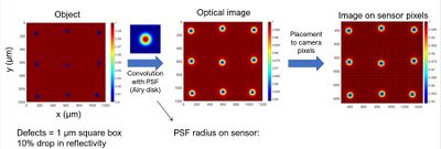
In our project, we take a simplistic approach and consider only changing the pixel size while keeping other parameters like camera noise performance, quantum efficiency, and illumination constant. A simple microscope is simulated using a 10X objective with NA=0.5, 200mm tube lens and monochromatic illumination of 550 nm. We assume the illumination flux on the sensor is 100 photons/s/u. The FOV at the sensor plane is 2000 um by 2000 um, and we vary the pixel size from 5um to 12um to determine the optimal pixel size for our defect of interest.
Our defects of interest are 1um by 1um squares (400 of them), with a relative reflectivity that is 10% lower than the background. The defects are placed on a 10um square grid, and a +/- 1um shift in both directions to randomise the defects.
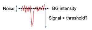
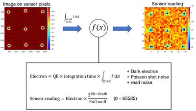
To simulate an optical image, the perfect defect image is convolved with a generated PSF. Noise and sensor read out is simulated to produce a sensor image. Using this sensor image, the detection algorithm is applied to determine which are defects or not. The detection is based on a simple thresholding algorithm by taking the intensity difference between the defect and the background. The background is calculated by taking the mean of the image at the edges where there are no defects. If the signal intensity is larger than the set threshold, it is classified as a defect. In our simulation, we used a threshold of 1000 DN.
The capture rate of the system can be then calculated: Capture Rate = (detected defects)/(total number of defects)
A high capture rate is desirable for a defect inspection system.
Results
Background intensity and noise vs. pixel size
From result of our simulation model, background intensity increases quadratically to the pixel size. This is expected as area increases quadratically to the pixel size as well.
Background noise increases linearly to the pixel size. This is also expected since number of photon collected is proportional to the area.
Capture rates when the pixel size and effective defects size match
Sensor with 7um pixels
Sensor with 10um pixels
Sensor with 11.4um pixels
Conclusions
We have successfully established a simulation model for brightfield defect detection microscopy for semiconductor application. Moreover, for the system used for our simulation model, we have found that detection is optimized when the pixel size matches with the defect of interest.
For future works, out simulation model could use different illumination that can be varied per pixel size to achieve specific gray level. Our scope could be also expanded to compute contributions from other parameters.
Appendix
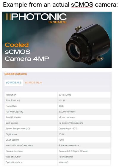
Camera parameters, taken from Photonic Science.
