EspositoWang: Difference between revisions
imported>Projects221 |
imported>Projects221 |
||
| Line 82: | Line 82: | ||
=== Simulations === | === Simulations === | ||
Various simulations in LTSpice were performed prior to and in parallel with testing the prototype breadboarded version. The idea was to use the same circuit configuration as in the previous project since the MOSFET and BJT current limits the maximum amount of current through the LED. The optimal feedback resistance (in series with MOSFET source) was found by adjusting the resistance so the current in the saturation region of the MOSFET was approximately 1A. The feedback resistor has to be rated for at least 3 watts to handle the 1A. Lower power rating resistors could be used since the LED flash system will not have a continuous 1A flowing through it, the flash duration will be within the range of ~10ms or less. | Various simulations in LTSpice were performed prior to and in parallel with testing the prototype breadboarded version. The idea was to use the same circuit configuration as in the previous project since the MOSFET and BJT current limits the maximum amount of current through the LED. The optimal feedback resistance (in series with MOSFET source) was found by adjusting the resistance so the current in the saturation region of the MOSFET was approximately 1A. The feedback resistor has to be rated for at least 3 watts to handle the 1A. Lower power rating resistors could be used since the LED flash system will not have a continuous 1A flowing through it, the flash duration will be within the range of ~10ms or less. | ||
<br> | |||
The feedback resistor value is 0.68ohms, while the resistor on the collector side of the BJT was 51ohms. The MOSFET model used in the simulation was the FQP20N06L, but in the actual circuit we used the FQP30N06L. Fairchild Semiconductors did not make a FQP30N06L model so we used the closest model as possible. Although the values for the resistors were obtained through simulations, we knew that once we tested the actual circuit, we would have to modify the resistor on the collector side of the BJT to compensate for the difference in the MOSFET models. | The feedback resistor value is 0.68ohms, while the resistor on the collector side of the BJT was 51ohms. The MOSFET model used in the simulation was the FQP20N06L, but in the actual circuit we used the FQP30N06L. Fairchild Semiconductors did not make a FQP30N06L model so we used the closest model as possible. Although the values for the resistors were obtained through simulations, we knew that once we tested the actual circuit, we would have to modify the resistor on the collector side of the BJT to compensate for the difference in the MOSFET models. | ||
<br> | |||
As shown in the figures below, the circuit simulation for the LEDs only consisted of the LED driver current and not the charging/discharging unit. All the LEDs on the LED module were simulated except for the deep red and red LEDs because models were not available for those components. | As shown in the figures below, the circuit simulation for the LEDs only consisted of the LED driver current and not the charging/discharging unit. All the LEDs on the LED module were simulated except for the deep red and red LEDs because models were not available for those components. All simulation files can be found in the Appendix. | ||
<br> | |||
NOTE: The charging/discharging system was not simulated because models for the LM317 from Texas Instruments were not available and for some reason simulating capacitors in the Farad (1-50F) range does not simulate properly in LTSpice. | NOTE: The charging/discharging system was not simulated because models for the LM317 from Texas Instruments were not available and for some reason simulating capacitors in the Farad (1-50F) range does not simulate properly in LTSpice. | ||
Revision as of 01:14, 17 March 2013
Back to Psych 221 Projects 2013
LED Flicker Super Capacitor Design
Background
This projects builds upon the 2012 LED Flicker project. Instead of controlling the LEDs via PWMs, which has properties of flicking between OFF and ON states, the goal of this project is to design a system that provides a constant current through each LED. The design will mimic a camera flash with the use of super capacitors and a benchtop power supply or power supply wall adapter to flash each LED with 1 amp of current. There are 7 different LEDs on the LED array module and each LED must be flashed so that no two LEDs are on at the same time. The amount of time duration that the LED is on and the time interval between LED flashes are adjustable to allow for ease of use. Modifications can be made so that this design can be used with Alkaline or Lithium-Ion batteries to make the entire system compact and portable.
High Level Device Specifications
- Should have at least 7 channels for controlling each LED
- The rate at which the LEDs flash should be adjustable
- To adjust the interval time between each LED flash and the duration that each LED is on for
- The light intensity shall be constant and be set with ~1A of current
- Easy modifications can be made so that the light intensity can be adjustable
- System design should be modular to allow for quick modifications to system parameters
- Amount of charge caps can hold the amount of current through LED
- Should incorporate the use of super capacitors for a quick discharge of energy to the load
Device Overview
Design
Components
- LED Array of primary lights
- For the final design : 7-in-1 round assembly LED Array
- Arduino Uno microcontroller product
- A circular flat top Heat Sink Diameter ~ 2 1/4th inches
- A perforated circuit board (for the intermediate design) and a breadboard (for making a prototype)
- Circuit components
- 50F super capacitors product
- Fairchild Semiconductor FQP30N06L: N-Channel MOSFET datasheet
- Fairchild Semiconductor 2N3904 NPN BJT datasheet
- TI LM317 Adjustable Linear Regulator datasheet
- Ohmite RA-T2X-51E Heatsink, TO-220 product
- Assmann WSW Heatsinks, TO-220 product
- Kyoto Solid State Relay: In-32VDC max, Out-60VDC max, 4A max datasheet
- 1.3 Ohm 5% 3 watt power resistors feedback resistances
- 2.7KOhm 5% 1/4 watt resistors to connect control signals from the Arduino to the circuit.
LED Driver Circuit

To get a system that produces a stable light output, the LED must be driven by a constant current. An approach to get a constant current is using the circuit to the right. The way this circuit works is that the feedback resistor and BJT combination sense the amount of current flowing though the LED and feed this signal back to the MOSFET gate controlling its voltage and hence the current flowing through it. This design allows approximately ~1A of current to flow through the LED. The key idea was to operate the MOSFET within it's saturation region so the drain current flowing would not be disrupted by any change in the drain-source voltage above it's saturation cutoff value. Simulations were performed to determine the cutoff regions for the parts that were used.
The key parameter that must be selected with caution is the feedback resistance since that controls the maximum amount of current flowing through the circuit. Since high amounts of current will be flowing through the resistor, it is important that the resistor can handle the current, so power resistors must be used to dissipate the amount of power across it. To determine what feedback resistance we needed, we performed some simulations in LTSpice to verify that the circuit will work the way we believe it does and what the optimal resistance is for the feedback and for the resistor on the collector side of the BJT.
Seven copies of this circuit will be made to drive each LED, with the seven MOSFET enable signals routed from the Arduino microcontroller.
Super Capacitor Charging/Discharging Circuit

Quick overview of the circuit...
NOTE: Need to incorporate why we used the MOSFET in the saturation region (as stated in the section above), and how we made the voltage on the caps like 2-3 volts higher than the saturation cutoff region to make the circuit have enough charge to perform the flash sequence a few times.
BLAH
BLAH
BLAH
BLAH
BLAH
BLAH
BLAH
BLAH
Overall System Design
The entire circuit design is shown below. Since there are 7 LEDs on the LED array module, each of the individual LED driver circuits is connected at the same node (in parallel).

Method
Simulations
Various simulations in LTSpice were performed prior to and in parallel with testing the prototype breadboarded version. The idea was to use the same circuit configuration as in the previous project since the MOSFET and BJT current limits the maximum amount of current through the LED. The optimal feedback resistance (in series with MOSFET source) was found by adjusting the resistance so the current in the saturation region of the MOSFET was approximately 1A. The feedback resistor has to be rated for at least 3 watts to handle the 1A. Lower power rating resistors could be used since the LED flash system will not have a continuous 1A flowing through it, the flash duration will be within the range of ~10ms or less.
The feedback resistor value is 0.68ohms, while the resistor on the collector side of the BJT was 51ohms. The MOSFET model used in the simulation was the FQP20N06L, but in the actual circuit we used the FQP30N06L. Fairchild Semiconductors did not make a FQP30N06L model so we used the closest model as possible. Although the values for the resistors were obtained through simulations, we knew that once we tested the actual circuit, we would have to modify the resistor on the collector side of the BJT to compensate for the difference in the MOSFET models.
As shown in the figures below, the circuit simulation for the LEDs only consisted of the LED driver current and not the charging/discharging unit. All the LEDs on the LED module were simulated except for the deep red and red LEDs because models were not available for those components. All simulation files can be found in the Appendix.
NOTE: The charging/discharging system was not simulated because models for the LM317 from Texas Instruments were not available and for some reason simulating capacitors in the Farad (1-50F) range does not simulate properly in LTSpice.
- Simulation waveforms
-
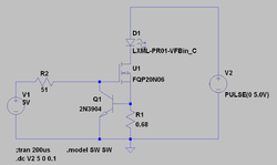 Royal Blue (447.5nm) LED circuit (without super caps)
 -
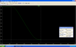 Royal Blue LED current waveform
 -
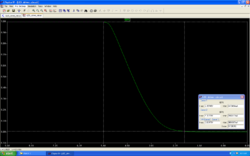 Blue (470nm) LED current waveform


Characterization of LED Array Module
Although simulations were performed for the LED driver circuit with averaged models of the Luxeon LEDs, we wanted to fully characterize the LEDs ourselves to determine how much of a difference there was from the model to the actual product. To test each LED, we hooked each one within the LED driver circuit to a benchtop power supply with initially 0V. We stepped up the voltage by 0.1V and made note of what the current draw from the LED was. As you can see, the measured plot is very similar to the simulated plots (royal blue LED shown below). The major noticeable difference is from 2.7-3.6V range in which the shows a very weird effect from the LEDs. At around 3.5-3.6V (which is very close to the voltage drop of the LED), the LED suddenly kicks on and conducts hard. If the upper linear portion of the plot is extrapolated down, it would look more like the simulated.
One difference between the simulated and measured plots is that the MOSFET was different. The actual MOSFET was an FQP30N06L while the simulated MOSFET was a FQP20N06L (fairchild semiconductor did not have a model for the FQP30N06L). From the simulation, the current in the saturation mode is ~1A, but when measured and due to the difference of the MOSFETs, the resistor value on the collector side of the BJT was 51 ohms in the simulation made the measured saturation current limit at 1.1-1.2A. To make sure that the limit of ~1A is strictly enforced, the resistor was changed to 2.7K. Tests were conducted and the LEDs were clamped to 1A within a +/-0.5% range.
From this test, we were able to observe that the average saturation cutoff region for all the LEDs is around 4.8V. For the flash sequence to run a few times before the capacitors have to be charged fully again, 2-3 volts + 4.8V across the capacitors should be sufficient. Data from all LED characterization can be found in the Appendix.
- Breadboard Circuits
-
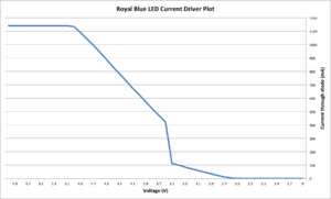 Royal Blue LED current plot
 -
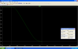 Simulated results

Super Capacitor Charging/Discharging Design Testing
Section for Bill
Discuss about how the works and was tested...Video of the charging/discharging with arduino sensing is in the appendix
Prototype Circuit
As a prototype for the final circuit, we designed the system on a breadboard. The circuits for each of the seven channels feeding the individual LEDs were small and compact. We modified the existing firmware to parametrize the number of output channels. Once the circuit was ready we connected it to the arduino and gave commmands to the Arduino through the USB port serial interface.
- Breadboard Circuits
-
 LED driver circuit on breadboard
 -
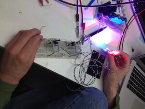 LED driver circuit testing


Intermediate Design
An intermediate version of the circuit was designed on a perforated circuit board using the 7 LED round-assembly configuration Luxeon LEDs. The purpose of this design was to run the system under actual operating conditions to verify that all the used circuit element ratings were appropriate for operation. Basically, check whether there were any faults like overheating in specific components.
The LED assembly was fastened with screws on to the flat round surface of the metallic heat sink, and separated by a thin layer of Heat Sink Paste. Wires were soldered onto the terminals of each LED. I color coded the wires as orange to represent positive and white to represent negative, for consistency. The perforated circuit board that I used had dimensions 7.5"x5.5" but this was larger than necessary. The heat sink average circular diameter was 2 5/16ths inch and so I used a hole saw of diameter 2 1/4ths inch to drill a hole in the middle of the circuit board to make the heat sink with the LED Assembly fit neatly through. I arranged and soldered all the circuit components in a circle around the central hole for compact connections to the LEDs.
All the individual circuit grounds were short-circuited and a common ground wire was exposed. Similarly all the positive terminals of the LEDs were short circuited and a common Vdd wire was exposed. The common ground and common Vdd were connected to a female Barrel connector terminal. The barrel connector was connected to the power supply using a standard power adapter. The Adapter specifications were Input: 100-240V 1A 50-60Hz, Output: 5V, 4A DC. The connector was a standard 2.5mm(ID)-5.5mm(OD) connector.
For each individual circuit the PWM signal input port was connected to a wire obtained from stripping an Ethernet Coaxial cable. The reason for this choice was because they could be easily wound together and made to emerge from the unit as a compact collection. The ends of the wires were soldered onto the pins of DIP male connectors so that they could just be slid into the Arduino connection sockets. To prevent the soldered wires from short-circuiting Heat Shrink was used to insulate exposed connections.
At this stage the Pins on the Arduino that were configured to provide the digital PWM output were (Digital) Pins 2,3,5,6,11,12,13.

Trade Offs
Trade off between charging time and efficiency....
Battery Design Considerations
Once the super caps were tested with a bench top power supply, we decided to test the caps charging and discharging time in the same configuration but with a 9V alkaline battery. A 9V battery performance is characterized by milliamp-hours capacity. As shown in the characteristic graphs below, for an energizer max 9V alkaline battery, with a discharge of 500mA, the capacity of the battery is approximately 300mAh. With the discharge trend, a discharge of 1A would have approximately 250mAh of capacity, giving the life of the battery to only 15 minutes for a continuous load of 1A. The 9V characteristic curves as shown below also indicate that the estimated 15 minutes of battery life for the system is an overestimation.
- Energizer Max 9V Alkaline Battery Performance Curves
-
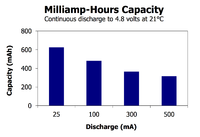 9V battery mAh capacity
 -
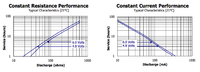 9V battery characteristic curves


Arduino Code Development
Code development methodology...
Results
Results section.....
Conclusions
Conclusions?
References
Appendix I - Code and Data
Files
LTSpice code for simulated circuit: File:LED driver simulations.zip
- Need to install MOSFET and LED models to work properly
Altium Designer schematics: File:Altium Schematics.zip
LED characterization data tables: File:LED characterization data.zip
Arduino code for driving LED circuit: [[File:]]
Prototype Data
Video of LED driver circuit test: File:LED driver testing.zip
Video of super capacitor charging/discharging with Arduino voltage sensing: File:Arduino sensing cap voltage.zip
Appendix II - Work partition
Simulation development - David Wang
Hardware assembly - William Esposito, David Wang
Firmware development - William Esposito